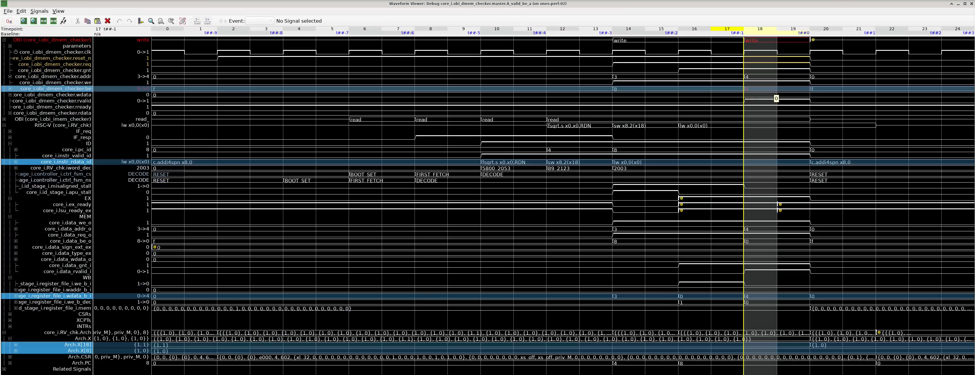
OBI R-7 and R-8 violations
Created by: salaheddinhetalani
Issue Description
OBI R-7 and R-8 rules are violated by misaligned memory instructions causing multiple memory accesses in case they are preceded by a multicycle F instruction, as they set the wrong byte enable value during the second memory access.
Component
Component:RTL
OBI Specification
R-7: The be values during the address phase of a transaction shall be as follows: At least one of the be bits shall be set to 1. The 1’s in be shall be contiguous.
R-8: The least significant addr bits shall be consistent with the be value during the address phase of a transaction, i.e.: If i is the index of the least significant bit in be that is 1, then the least significant addr bits shall be <= i
RISC-V Specification
The Zfinx extension adds all of the instructions that the F extension adds, except for the transfer instructions FLW, FSW, FMV.W.X, FMV.X.W, C.FLW[SP], and C.FSW[SP].
The Zfinx variants of these F-extension instructions have the same semantics, except that whenever such an instruction would have accessed an f register, it instead accesses the x register with the same number.
Steps to Reproduce
As shown below, the following sequence of instructions happens:
fsqrt.s x0, x0, RDN -> sw x8, 2(x18) -> lw x0, 0(x0)
The store instruction sets its first memory access at t##-2 correctly, setting the address to 32'h3 and the byte enable signal to 4'h8. The violation happens in the store's second memory access at t##0, where the byte enable signal is set wrongly to 4'h0 instead of the right value of 4'h1.
Top Level Parameters
cv32e40p_wrapper #(
    .PULP_XPULP       (0),
    .PULP_CLUSTER     (0),
    .FPU              (1),
    .PULP_ZFINX       (1),
    .NUM_MHPMCOUNTERS (1)
)
Git Hash: https://github.com/openhwgroup/cv32e40p/commit/d0d1c25374e3770c4335568ef16e84404cedbdea Flist: cv32e40p_fpu_manifest.flist VCD: bug_0.vcd
Product: OneSpin 360 DV-Verify App: Processor Verification App Tool's version: 2022.3_1
